Foundry process developer expands wafer-fabrication facility

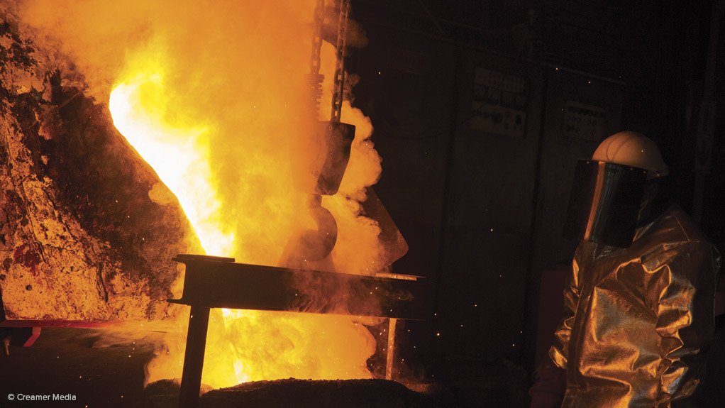
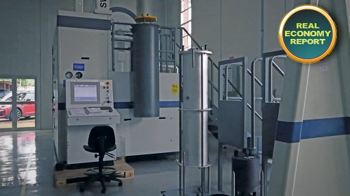
EXTENSIVE CAPABILITIES The foundry’s extensive process capabilities enable short manufacturing lead times while improving device yield and performance
Photo by Duane Daws
SpecialIty foundry process developer and fabricator Noel Technologies has expanded its wafer-fabrication facility in Silicon Valley by adding square footage and installing additional equipment that boosts its production capacity by 25%.
With additions including an i-line lithography system with 0.35 micron resolution, a top-down CD scanning electron microscope and more plasma- enhanced chemical vapor deposition tools, the 20-year-old company has increased its range of foundry services for customers in the semiconductor, microelectromechanical systems, biomedical device, sensor and light- emitting-diode markets.
“We perform many wafer- fabrication services integral to the development of the newest micro- and nanoelectronic products,” says Noel Technologies founder and chief technical officer Leon Pearce.
He adds that, as a manufacturing partner located in Silicon Valley, in California, the company can offer chip designers a local foundry solution to shorten their research and development cycles and reduce their time to production.
The full-service foundry combines high-quality process modules with the engineering expertise needed to help customers move seamlessly from custom design to device manufacturing.
All front-end wafer processing is performed in-house under the supervision of Noel Technologies’ experienced process engineering team, eliminating the need for customers to coordinate work flows among multiple suppliers. The foundry’s extensive process capabilities enable short manufacturing lead times while improving device yield and performance.
In fabricating a variety of devices, Noel Technologies routinely deposits thin-film dielectrics for three main purposes. The first being passivation layers to insulate or isolate active areas, the second hermetic layers between active areas to improve long-term reliability, and thirdly, in the case of dielectrics such as low-pressure chemical vapor deposition nitride, to provide electrical components such as breakdown voltage layers for power devices.
The company also deposits thin-film metals to create an array of sheet resistance values, which designers can use in tuning the electrical characteristics of each device design. In addition, Noel Technologies’ lithography and etching services enable precise control of devices’ topographies.
The company also explains that, owing to the multibillion- dollar cost of building and operating a wafer-fabrication facility, the vast majority of semiconductor companies focus on device design and do not have the resources to manufacture products. These companies rely on partners for foundry manufacturing services.
While large foundries provide fabrication services using standard complementary metal– oxide–semiconductor (CMOS) processes, Noel Technologies specialises in helping chip designers that work with advanced non-CMOS materials and nonstandard process flows.
The company adds that it has decades of experience and proven capabilities in developing novel process flows involving III-V compound materials such as gold, silver, transparent conductive oxides and emerging materials.
Unlike integrated device manufacturers with excess production capacity that offer foundry services, Noel Technologies explains that it does not produce its own devices and does not retain chip designers’ Internet protocol. This business model helps to safeguard fabless customers from undue risk.
Article Enquiry
Email Article
Save Article
Feedback
To advertise email advertising@creamermedia.co.za or click here
Announcements
What's On
Subscribe to improve your user experience...
Option 1 (equivalent of R125 a month):
Receive a weekly copy of Creamer Media's Engineering News & Mining Weekly magazine
(print copy for those in South Africa and e-magazine for those outside of South Africa)
Receive daily email newsletters
Access to full search results
Access archive of magazine back copies
Access to Projects in Progress
Access to ONE Research Report of your choice in PDF format
Option 2 (equivalent of R375 a month):
All benefits from Option 1
PLUS
Access to Creamer Media's Research Channel Africa for ALL Research Reports, in PDF format, on various industrial and mining sectors
including Electricity; Water; Energy Transition; Hydrogen; Roads, Rail and Ports; Coal; Gold; Platinum; Battery Metals; etc.
Already a subscriber?
Forgotten your password?
Receive weekly copy of Creamer Media's Engineering News & Mining Weekly magazine (print copy for those in South Africa and e-magazine for those outside of South Africa)
➕
Recieve daily email newsletters
➕
Access to full search results
➕
Access archive of magazine back copies
➕
Access to Projects in Progress
➕
Access to ONE Research Report of your choice in PDF format
RESEARCH CHANNEL AFRICA
R4500 (equivalent of R375 a month)
SUBSCRIBEAll benefits from Option 1
➕
Access to Creamer Media's Research Channel Africa for ALL Research Reports on various industrial and mining sectors, in PDF format, including on:
Electricity
➕
Water
➕
Energy Transition
➕
Hydrogen
➕
Roads, Rail and Ports
➕
Coal
➕
Gold
➕
Platinum
➕
Battery Metals
➕
etc.
Receive all benefits from Option 1 or Option 2 delivered to numerous people at your company
➕
Multiple User names and Passwords for simultaneous log-ins
➕
Intranet integration access to all in your organisation


